Every photonic integrated circuit — every splitter, ring, filter and coupler — is built from one primitive: a waveguide carrying a guided mode. Get the waveguide layer right and the components above it behave; get it subtly wrong and the whole chip inherits the error. Most "mysterious" PIC failures we audit trace back not to exotic physics but to waveguide-level decisions made by default instead of by design.
The one number that runs the show: effective index
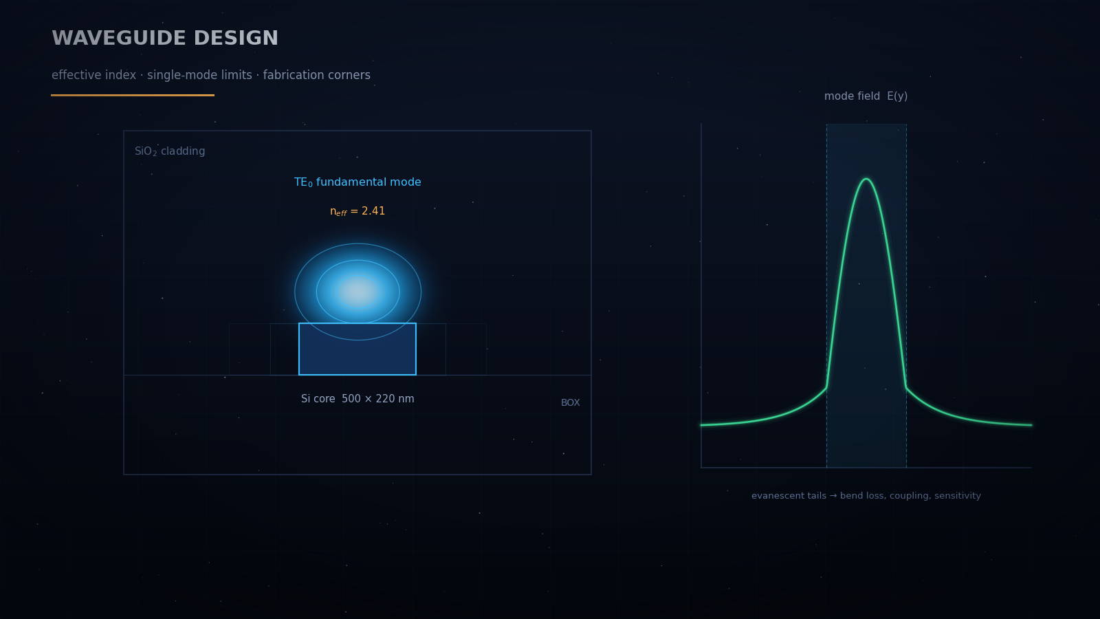
A guided mode doesn't travel at the speed set by the core material or the cladding — it travels at a speed set by its effective index, n_eff, a weighted answer to the question "how much of this mode actually lives in the core?" Everything an engineer cares about is a derivative of n_eff:
- Phase and path matching. Interferometers, ring resonances and WDM filters are all phase devices; their function is literally an n_eff × length product.
- Dispersion. How n_eff changes with wavelength sets FSR drift, pulse behavior and filter bandwidths.
- Coupling. Directional couplers work by the beat between the n_eff of two supermodes; get either wrong and your 50/50 splitter ships as a 62/38.
- Sensitivity. How strongly n_eff responds to width, thickness and temperature is the device's tolerance behavior.
A standard 500 × 220 nm silicon strip waveguide at 1550 nm has an n_eff near 2.4 — comfortably between silicon (~3.48) and oxide (~1.44), exactly as the "how much lives in the core" picture predicts.
The single-mode boundary is a design decision
Make the core too small and light escapes to radiation; too large and it guides multiple modes, each with its own n_eff — turning your neat phase device into an interference lottery. The single-mode window is the fundamental trade of the layer:
- Near the multimode edge (wider): lower loss, weaker sidewall interaction, gentler sensitivity — but a stray taper or bend can excite mode two.
- Near cutoff (narrower): tighter confinement of the fundamental... until the mode swells into the cladding, loss climbs, and everything becomes exquisitely sensitive to geometry.
Real designs place different waveguide widths in different circuit regions — routing wide, bending and coupling at reference width — with adiabatic tapers negotiating between them. Choosing those widths is eigenmode analysis, not folklore.
Bends: where the loss budget goes to die
Straight-waveguide propagation loss gets the datasheet glory, but circuits are mostly corners. Bend a waveguide and the mode leans outward; bend it too tightly and it radiates. The bend radius that keeps loss negligible depends steeply on confinement — a silicon strip guide tolerates ~5 µm radii; the same layout instinct on a weakly-confining platform can bleed decibels per turn. Add the transition loss where straight meets curve (the mode centers don't line up), and a dense layout accumulates hundreds of these small penalties. Budgeting them is bookkeeping — the kind a mode solver does exactly and intuition does optimistically.
The fab always votes: corners are the real spec
The wafer will not deliver your nominal geometry. Width shifts with lithography and etch bias; thickness varies across the wafer; sidewalls slope. On a standard silicon platform, a ±10 nm width excursion is a realistic process window — and it moves n_eff enough to shift a ring resonance by more than a channel spacing, or walk a coupler visibly off its ratio.
This is why we treat corner analysis as the integrated-photonics tolerance budget: sweep width, thickness and etch depth over the platform's stated window; watch n_eff, coupling ratio, resonance and loss respond; then either center the design, desensitize the geometry (wider single-mode guides where possible, adiabatic rather than resonant structures), or add tuning and calibration deliberately. A component library with corner curves attached is worth ten libraries of nominal spectra.
Simulate like you mean it
The workflow that survives contact with the foundry: eigenmode analysis for everything translationally uniform — n_eff, dispersion, bend loss, coupling lengths — because it is fast and exact for that geometry; 3-D full-wave (FDTD) verification for everything that scatters — grating couplers, junctions, tapers, crossings — where mode theory stops being the whole story; and corner sweeps wrapped around both. Component design without variation analysis isn't finished design; it's a good day in the simulator.
The takeaway
Waveguide design looks like the easy part of photonics precisely because the decisions are quiet: a width here, a radius there, a taper length nobody reviews. Those quiet decisions set the noise floor for every device above them. If your chip's measured spectra drift, split unevenly or lose light you can't account for — start the audit at the waveguide layer. That's where we start, and it's where the answer usually is.
Want to build intuition first? Try our free in-browser slab waveguide mode solver in the engineering tools — real dispersion equations, live field profiles.
Have a similar engineering challenge? Talk to our optical engineers — a fixed-scope diagnostic turns uncertainty into a costed plan, typically within weeks.