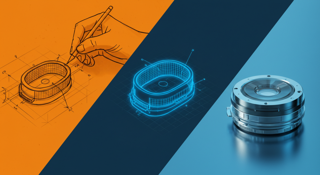
From Concept to Production: The Journey of Custom Optics Design
In today’s technology-driven world, optics play a crucial role in countless applications, from smartphones to medical devices. But how does an optical design transform from an idea into a finished product? This article provides a step-by-step overview of the custom optics design process, presented in a way that both technical professionals and non-specialists can appreciate.
1. Defining the Requirements
The first step in any design process is understanding the requirements. For custom optics, this involves answering questions like:
- Application of the optic: Understanding whether the optic will be used for imaging, illumination, laser delivery, or another purpose is critical for determining its properties and constraints.
- Performance criteria: This includes parameters such as resolution (sharpness), field of view (the area captured or illuminated), transmission efficiency, and wavelength range.
- Physical and environmental constraints: Size, weight, temperature tolerance, and exposure to dust or moisture influence material and design choices.
Detailed technical specifications, often documented in a requirements specification sheet, serve as a foundation for the design process. Teams may use tools like Quality Function Deployment (QFD) to prioritize and align on these requirements.
2. Concept Development
With the requirements defined, designers move into the brainstorming phase, leveraging advanced optical design software like Zemax OpticStudio or Synopsys Code V. During this phase, the following aspects are considered:
- Lens shapes and materials: Material selection involves evaluating refractive indices, dispersion, and thermal properties. Specialized glasses or plastics may be used for unique applications.
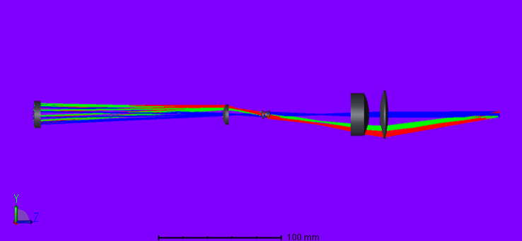
- System layout: Initial concepts outline the placement and alignment of lenses, mirrors, prisms, and apertures. This stage often includes sketching ray diagrams to visualize light propagation.
- Initial simulations: Basic ray tracing simulations help identify potential optical aberrations or inefficiencies early on, saving time in later stages.
The goal is to generate several viable concepts that balance performance, manufacturability, and cost. Collaboration across disciplines, including mechanical and electronic engineering, ensures the concepts are practical and robust.
3. Detailed Optical Design
Once a promising concept is selected, the design enters a detailed optimization phase, which is both iterative and data-intensive. Key tasks include:
- Aberration correction: Advanced mathematical models and simulation tools are used to address spherical, chromatic, and other optical aberrations. Techniques such as aspheric surfaces or diffractive optics may be introduced.
- Tolerance analysis: Manufacturing imperfections like surface irregularities or misalignments are inevitable. Monte Carlo simulations and sensitivity analyses help predict and mitigate their effects on performance.
- Thermal and mechanical robustness: Designs are evaluated for stability under varying temperatures and mechanical stresses. Thermal expansion coefficients and structural supports are modeled in tandem with the optical system.
Simulations form the backbone of this phase. They allow designers to predict system performance under various real-world conditions, enabling precise optimization before physical production begins. However, conducting and iterating on simulations can be resource-intensive. Partnering with an experienced optical design services company, such as MyntOptics, can significantly reduce this load. These experts leverage cutting-edge tools and methodologies to accelerate the design process, minimizing costs and ensuring optimal performance outcomes.
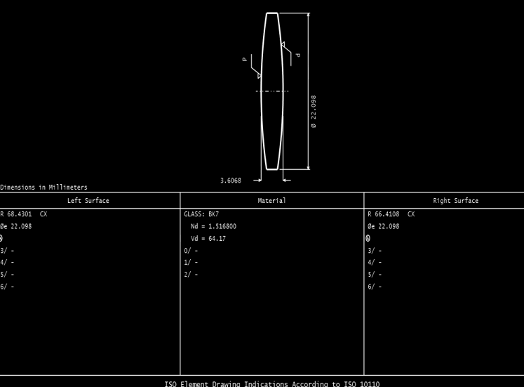
Drawings and Vendor Communication
Following detailed design and simulation, precise technical drawings are created in adherence to ISO standards for technical drawings. These drawings include lens specifications, material details, tolerances, and assembly instructions. They serve as the primary communication tool with manufacturing vendors, ensuring all design intent is accurately conveyed. Vendors use these drawings to produce prototypes or final components with exacting precision. Sharing detailed design information also enables early identification of manufacturability challenges, streamlining the transition to production.
4. Prototyping and Testing
After the design is finalized, prototyping and production are typically entrusted to specialized manufacturing vendors. This involves:
- Vendor selection: Identifying manufacturers with expertise in optical fabrication and assembly, ensuring they can meet tight tolerances and specifications.
- Fabrication: Vendors employ precision grinding, diamond turning, injection molding, or even additive manufacturing to produce components. Coatings such as anti-reflective or mirror finishes may also be applied.
- Assembly: Optical components are mounted and aligned in housings designed to minimize stray light and ensure durability. Advanced alignment tools and techniques, like laser alignment, are often used.
- Testing: Vendors conduct rigorous optical tests, including interferometry, MTF (Modulation Transfer Function) measurement, and environmental stress testing. Collaborating with the design team ensures the prototype meets or exceeds performance benchmarks.
Feedback from testing may necessitate design tweaks, creating a feedback loop until the prototype achieves desired outcomes.
5. Transition to Production
When the prototype is validated, the focus shifts to scaling the design for production. Key considerations include:
- Mass production methods: Techniques such as injection molding for plastic optics or CNC machining for glass optics are optimized for cost and speed without sacrificing quality.
- Quality assurance protocols: Inspection processes, including automated optical inspection (AOI) and statistical process control (SPC), are implemented to ensure consistency across production batches.
- Supply chain logistics: Collaboration with material suppliers and subcontractors ensures timely delivery and cost efficiency. Packaging solutions are designed to protect optics during transport and storage.
Designers may also document manufacturing processes and specifications to enable seamless production handovers.
6. Deployment and Support
The first step in any design process is understanding the requirements. For custom optics, this involves answering questions like:
- Application of the optic: Understanding whether the optic will be used for imaging, illumination, laser delivery, or another purpose is critical for determining its properties and constraints.
- Performance criteria: This includes parameters such as resolution (sharpness), field of view (the area captured or illuminated), transmission efficiency, and wavelength range.
- Physical and environmental constraints: Size, weight, temperature tolerance, and exposure to dust or moisture influence material and design choices.
Bridging the Gap Between Science and Application
Custom optics design is a blend of art and science. It requires creativity to envision solutions, technical expertise to refine them, and practical considerations to bring them to market. By following a structured process from concept to production, optical designers can create systems that drive innovation and solve real-world challenges.
At MyntOptics, we take pride in supporting this transformative journey. With our extensive expertise in optical design, simulation, and collaboration with top-tier manufacturing vendors, we deliver solutions tailored to your unique needs. To learn more about how MyntOptics can bring your vision to life, visit MyntOptics.com. Whether you’re a business leader exploring custom optics for your next product or a curious enthusiast, understanding this process sheds light on the fascinating journey of turning ideas into impactful technologies. If you’d like to learn more or discuss potential projects, feel free to connect and start a conversation!
#Optical Design #Optics Consulting #OpticalEngineeringServices